Processing

Silicon wafer process development

How to develop a design to a mass-produced product? At Kyocera Technologies, our MEMS processing methods are the result of a long, groundbreaking development.

Tools and expertise

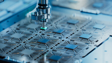
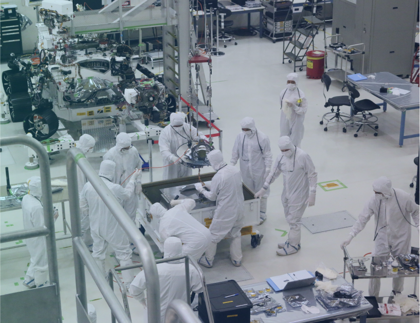
Once the component design is created, then the product is processed with multiple different types of processing equipment. Being able to extend the use of silicon in new areas, such as MEMS resonators as timing devices, has necessitated the development of new methods and practices.

The power of partner network

We do our processing work mostly at the Micronova facility in Otaniemi where we are located, but we use also internal and external partner network as needed to perform these tasks.

Focus on the production

The processes created for the products in our R&D are later transferred to manufacturing. This means that we need to focus on things such as manufacturing yield to make sure the mass production will be efficient.

Work with us

Ready to join the revolution?

What unites our team consisting of over 10 nationalities and working closely with our sister team in Japan? Part of it is the thrill of creating cutting-edge technology – being a part of the revolution. But it is also the team spirit, the appreciation of different people from different backgrounds as individuals. If you are one of the best and the brightest, you might have what it takes to rock the boat with MEMS technology.

LEARN MORE AND JOIN OUR TEAM!